TL866 II PLUS: Difference between revisions
(Created page with "Category:TL866 Category:Hardware Category:Programmer The TL866 II PLUS is '''NOT''' compatible with the TL866 A / TL866 CS models. The microcontroller has been c...") |
(→Pinouts: add IO expander pin mappings) |
||
| (5 intermediate revisions by 2 users not shown) | |||
| Line 3: | Line 3: | ||
[[Category:Programmer]] | [[Category:Programmer]] | ||
The TL866 II PLUS is '''NOT''' compatible with the TL866 A / TL866 CS models. The microcontroller has been changed to a | The TL866 II PLUS is '''NOT''' compatible with the [[TL866|TL866 A / TL866 CS]] models. The microcontroller has been changed from a PIC18 to a PIC24F and there are other significant schematic changes. The plastic enclosure for the TL866 II PLUS is identical to the TL866A / TL866CS. | ||
The | = Hardware = | ||
The TL866II PLUS is driven by a Microchip [https://www.microchip.com/wwwproducts/en/PIC24FJ256GB110 PIC24FJ256GB110] microcontroller which connects directly to the USB. | |||
[[:Media:TL866II_Schematic.pdf|Reverse-Engineered Schematic]] | |||
== Pinouts == | |||
{| class="wikitable" style="float: right; margin-left: 10px; text-align: center;" | |||
|+ ZIF40 Pinout | |||
! V<sub>PP</sub> !! V<sub>DD</sub> !! GND !! IO !! !! !! IO !! GND !! V<sub>DD</sub> !! V<sub>PP</sub> | |||
|- | |||
| RF1 || 0.00 || 0.0 || RD10 | |||
! 01 !! 40 | |||
| RD0 || 3.7 || 1.15 || 0.15 | |||
|- | |||
| RF0 || 0.01 || 0.1 || RD9 | |||
! 02 !! 39 | |||
| RD11 || 3.6 || 1.14 || 0.14 | |||
|- | |||
| RD7 || 0.02 || 0.2 || RD8 | |||
! 03 !! 38 | |||
| RD1 || 3.5 || 1.13 || 0.13 | |||
|- | |||
| RD6 || 0.03 || 0.3 || RF8 | |||
! 04 !! 37 | |||
| RD2 || 3.4 || 1.12 || 0.12 | |||
|- | |||
| RD13 || 0.04 || 0.4 || RF2 | |||
! 05 !! 36 | |||
| RD3 || 3.3 || 1.11 || 0.11 | |||
|- | |||
| 0.00 || 0.05 || 0.5 || RF5 | |||
! 06 !! 35 | |||
| RD4 || 3.2 || 1.10 || 0.10 | |||
|- | |||
| 0.01 || 0.06 || 0.6 || RF4 | |||
! 07 !! 34 | |||
| RD5 || 3.1 || 1.09 || 0.09 | |||
|- | |||
| 0.02 || 0.07 || 0.7 || RD15 | |||
! 08 !! 33 | |||
| RG14 || 3.0 || 1.08 || 0.08 | |||
|- | |||
| 0.03 || 0.08 || 1.0 || RD14 | |||
! 09 !! 32 | |||
| RG12 || 2.7 || 1.07 || 0.07 | |||
|- | |||
| 0.04 || 0.09 || 1.1 || RA1 | |||
! 10 !! 31 | |||
| RG13 || 2.6 || 1.06 || 0.06 | |||
|- | |||
| || 0.10 || 1.2 || RA15 | |||
! 11 !! 30 | |||
| RG15 || 2.5 || 1.05 || 0.05 | |||
|- | |||
| || 0.11 || 1.3 || RA14 | |||
! 12 !! 29 | |||
| RE7 || 2.4 || 1.04 || | |||
|- | |||
| || 0.12 || 1.4 || RE0 | |||
! 13 !! 28 | |||
| RE6 || 2.3 || 1.03 || | |||
|- | |||
| || 0.13 || 1.5 || RE1 | |||
! 14 !! 27 | |||
| RE5 || 2.2 || 1.02 || | |||
|- | |||
| || 0.14 || 1.6 || RE2 | |||
! 15 !! 26 | |||
| RE4 || 2.1 || 1.01 || | |||
|- | |||
| || 0.15 || 1.7 || RE9 | |||
! 16 !! 25 | |||
| RE3 || 2.0 || 1.00 || | |||
|- | |||
| || || || RE8 | |||
! 17 !! 24 | |||
| RD12 || || || | |||
|- | |||
| || || || RF12 | |||
! 18 !! 23 | |||
| RA5 || || || | |||
|- | |||
| || || || RF13 | |||
! 19 !! 22 | |||
| RA4 || || || | |||
|- | |||
| || || RB2 || RA2 | |||
! 20 !! 21 | |||
| RA3 || RB3 || || | |||
|} | |||
The primary interface to the target device is a 40 pin ZIF (zero insertion force) socket. Digital IO at LVCMOS3.3 levels is supported direct to the MCU on every pin. Inputs above +3.3V will be clamped. The V<sub>DD</sub> bus can be switched to pins 1-16 and 25-40. The V<sub>PP</sub> bus can be switched to pins 1-10 and 30-40. The ground bus can be switched to pins 1-16, 20, 21, and 25-40. | |||
<div style="clear: both;"></div> | |||
== Original research == | |||
* [[TL866_II_PLUS/Bootloader]] | |||
= Photos = | = Photos = | ||
Latest revision as of 08:35, 3 February 2020
The TL866 II PLUS is NOT compatible with the TL866 A / TL866 CS models. The microcontroller has been changed from a PIC18 to a PIC24F and there are other significant schematic changes. The plastic enclosure for the TL866 II PLUS is identical to the TL866A / TL866CS.
Hardware
The TL866II PLUS is driven by a Microchip PIC24FJ256GB110 microcontroller which connects directly to the USB.
Pinouts
| VPP | VDD | GND | IO | IO | GND | VDD | VPP | ||
|---|---|---|---|---|---|---|---|---|---|
| RF1 | 0.00 | 0.0 | RD10 | 01 | 40 | RD0 | 3.7 | 1.15 | 0.15 |
| RF0 | 0.01 | 0.1 | RD9 | 02 | 39 | RD11 | 3.6 | 1.14 | 0.14 |
| RD7 | 0.02 | 0.2 | RD8 | 03 | 38 | RD1 | 3.5 | 1.13 | 0.13 |
| RD6 | 0.03 | 0.3 | RF8 | 04 | 37 | RD2 | 3.4 | 1.12 | 0.12 |
| RD13 | 0.04 | 0.4 | RF2 | 05 | 36 | RD3 | 3.3 | 1.11 | 0.11 |
| 0.00 | 0.05 | 0.5 | RF5 | 06 | 35 | RD4 | 3.2 | 1.10 | 0.10 |
| 0.01 | 0.06 | 0.6 | RF4 | 07 | 34 | RD5 | 3.1 | 1.09 | 0.09 |
| 0.02 | 0.07 | 0.7 | RD15 | 08 | 33 | RG14 | 3.0 | 1.08 | 0.08 |
| 0.03 | 0.08 | 1.0 | RD14 | 09 | 32 | RG12 | 2.7 | 1.07 | 0.07 |
| 0.04 | 0.09 | 1.1 | RA1 | 10 | 31 | RG13 | 2.6 | 1.06 | 0.06 |
| 0.10 | 1.2 | RA15 | 11 | 30 | RG15 | 2.5 | 1.05 | 0.05 | |
| 0.11 | 1.3 | RA14 | 12 | 29 | RE7 | 2.4 | 1.04 | ||
| 0.12 | 1.4 | RE0 | 13 | 28 | RE6 | 2.3 | 1.03 | ||
| 0.13 | 1.5 | RE1 | 14 | 27 | RE5 | 2.2 | 1.02 | ||
| 0.14 | 1.6 | RE2 | 15 | 26 | RE4 | 2.1 | 1.01 | ||
| 0.15 | 1.7 | RE9 | 16 | 25 | RE3 | 2.0 | 1.00 | ||
| RE8 | 17 | 24 | RD12 | ||||||
| RF12 | 18 | 23 | RA5 | ||||||
| RF13 | 19 | 22 | RA4 | ||||||
| RB2 | RA2 | 20 | 21 | RA3 | RB3 |
The primary interface to the target device is a 40 pin ZIF (zero insertion force) socket. Digital IO at LVCMOS3.3 levels is supported direct to the MCU on every pin. Inputs above +3.3V will be clamped. The VDD bus can be switched to pins 1-16 and 25-40. The VPP bus can be switched to pins 1-10 and 30-40. The ground bus can be switched to pins 1-16, 20, 21, and 25-40.
Original research
Photos
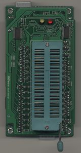
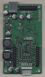
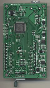
TL866 II PLUS photos
Photos of a TL866 II PLUS bought April 2018 from eBay seller goldenchipset.
Red and yellow LEDs were desoldered from mainboard to allow separation of the two PCBs.


