BPM WWAVUSBEPP
Background
At one point they sold an upgrade board to convert older programmers to USB. Basically what it boils down to is:
The adapter should work for BP-1400, BP-1600, BP-1700, and (some?) EPP series programmers You can swap it from one unit to another (ex: swap from BP-1410 to BP-1600 to upgrade an old unit) Units known to ship with this adapter * BP-1410 (probably BP-1610 and BP-1710 as well) * Silicon Sculptor 3 The adapter is no longer offered as an upgrade for the BP-1×00 models
http:www3.bpmicro.com/web/bphome.nsf/(web.news)/FB83F285AEE1E5BB862570670047820E
2.4 Mb/s to 9.0 Mb/s potential speed upgrade 14. What programming site models will this work with? * All EPP programmers. This encompasses 6th-gen and 7th-gen. * This may be a different adapter board 17. About how much will these adapters cost to make? * About $20 in materials 21. Why can’t I just buy an off-the-shelf USB-Parallel port adapter and use that? * There is no formal specification as to what you must do with these signals. Printer makers adhere to an informal standard as to what each of these signals does, but such functionality isn’t suitable for device programmers. * Even if the vendor-defined signals didn’t get in the way, the performance of any off-the-shelf adapter would be horrible (much worse than parallel port) 20. What are the Macola part numbers of the site adapter and the hub? * Site Adapter: WWAVUSBEPP * Hub: WWAVUSBHUB
https:www.febo.com/pipermail/time-nuts/2013-January/073818.html
>> All I have is an Actel Silicon Sculptor 3, also made by BP Micro,>> that looks like the BP-1710 (with the 'START' button) but connects>> via a USB port. On the main PCB of the BP-1600 and the SS3 are two,>> 2 row, 26 pin, connectors, one toward the back edge of the PCB toward>> the back panel and the other just inside the first connector. The>> inside connector directly connects to the parallel port on the back>> of the BP-1600. On the SS3, there is a small PCB that plugs into the>> same connector, takes a power input, and also has 6 pin connections>> to the other 26 pin connector. This small PCB has a USB connector>> that is> connected to the back of the SS3 as the USB connection.>>
Other:
It's part number is WWAVUSBEPP
From another doc:
> Automated Programming System users can determine if the handler is configured with the USB to EPP adapter through the PC Device Manager. If “BP Microsystems SPC Interface” is present as shown in the object below, then the USB to EPP adapter is already installed. If not, please contact BPM Microsystems Sales to order an upgrade kit part number: WHARUSBSPCKIT.
Programmer compatibility
Trying a 1600 with the adapter under 5.33.0 (last version to support parallel) worked fine. However, under 5.47.0 (newest release version as of today):
I analyzed the USB packet traces for kicks to see what was happening. There are some minor differences (ex: later software chunks firmware load up smaller) but otherwise they are identical in purpose. However, the newer software seems to just give up at one point. My guess is that they removed the 1600 handling code, not just the parallel interface to it.
CPCBD03223 Rev F (BP-1410)
Original unit was from
Power to J4
CPCB12A Rev C motherboard (BP-1600, SS2)
Connect to TERM 1 (J11). TERM 2 (J12) will not work)
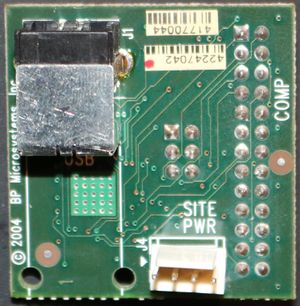
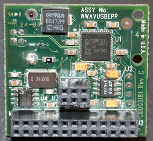
PCB overview
Above:
ASSY No. WWAVUSBEPP EPCBD03181 Rev C
Bpm:wwavusbepp:bpm wwavusbepp.png
Where
NOTE: a number of the component values above are best guesses. In particular:
R6/R7 divider Most small capacitors. T13/T17 are recommended values from cypress datasheet U3 is best guess
More info here: https:siliconpr0n.org/media/bpm/WWAVUSBEPP/
2015-04-24: tried plugging the adapter from my BP-1410 into my BP-1600 and it worked!
CY7C68013-
56LFC 0421
E 04
CYP 626381
KOR
U2 (?):
LT 515
176333
U3 (?):
U4 (8KB I2C EEPROM):
24C64W6
ST K414B
Pinout
| Pin | Dbg color | MCU pin | Function | PU/PD | |
|---|---|---|---|---|---|
| 1 | Black | 30: CTL1/FLAGB | |||
| 2 | Black | 29: CTL0/FLAGA | |||
| 3 | Brown | 18: PB0/FD0 | |||
| 4 | Brown | 34: PA1/INT1# | PU | ||
| 5 | Red | 19: FB1/FD1 | |||
| 6 | Red | 38: PA5/FIFOADR1 | |||
| 7 | Orange | 20: FB2/FD2 | |||
| 8 | Orange | 31: CTL2/FLAGC | |||
| 9 | Yellow | 21: PB3/FD3 | |||
| 10 | Yellow | N/A | GND | ||
| 11 | Green | 22: PB4/FD4 | |||
| 12 | Green | N/A | GND | ||
| 13 | Blue | 23: PB5:FD5 | |||
| 14 | Blue | N/A | GND | ||
| 15 | Violet | 24: PB6/FD6 | |||
| 16 | Violet | N/A | GND | ||
| 17 | Black | 25: PB7/FD7 | |||
| 18 | N/C | N/A | GND | ||
| 19 | Brown | 33: PA0/INT0# | PU | ||
| 20 | N/C | N/A | GND | ||
| 21 | Red | 1: RDY0/SLRD | PU | ||
| 22 | N/C | N/A | GND | ||
| 23 | Orange | 2: RDY1/SLWR | |||
| 24 | N/C | N/A | GND | ||
| 25 | Yellow | 35: AP2/SLOE | |||
| 26 | N/C | N/A | GND |
Resistor placed sub-optimially. is there another pullup?
17 signal pins, 16 LA channels. Arbitrarily drop pin 8 in favor of hooking everything up linearly.
2015-09-27
Project goal: understand how voltages/currents are read out
Phase 1: LA
Ran into some signal integrity issues setting up capture. Had to do short wires. More info:
Final setup * https:twitter.com/johndmcmaster/status/648329962819182592 * https:twitter.com/johndmcmaster/status/648348769746948097 Flaky: flying leads * https:twitter.com/johndmcmaster/status/648315944121425920 Complete failure: ribbon cable * https:twitter.com/johndmcmaster/status/645354861383385088
Setup to trigger on J2.1. Triggered during startup sequence reading serial number etc
Discovered Saleae only support 8/16 channels with USB 2. Ordered USB3 expresscard adapter.
SN:
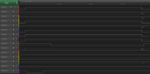
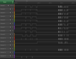
Above: 1-8 at startup
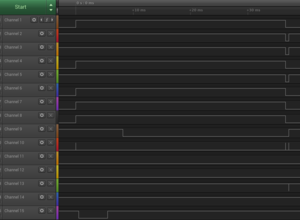
Above: after hitting don't register. 02_post_sn.lda
Above: after hitting okay that's in unsupported mode
Above: software started but idle
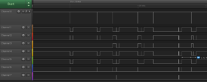
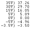
Above: voltage monitoring. 03_voltage.lda
Above also shows that signals are at least in the 1-1.25 MHz range. I'm currently sampling at 6.25 MS/s
Phase 2: USB cap/replay
Continue above project by toying with USB driver. Previously had some issue with certain response packet getting lost as it made its way back to the host (kernel capture: lost, libusb: lost, USB analyzer: received). This issue is what prompted this more detailed analysis. To that end, try to work in C to enable getting libusb help diagnosing the problem.
2015-09-29
Rewire Saleae cleaner. Confirmed that can select up to 500 MS/s with 2 channels with analog turned off
USB
VID: 14b9 PID: 0001
Looks like bp1410_sn.py (bfb0464a) demonstrates the issue I was having:
uvscada/bpm$ python bp1410_sn.py
Scanning for devices...
Found device
Bus 001 Device 006: ID 14b9:0001
val 157: 08160100
val 165: 000000
bulk read 167
Traceback (most recent call last):
 File "bp1410_sn.py", line 689, in <module>
   replay(dev)
 File "bp1410_sn.py", line 495, in replay
   buff = bulkRead(0x86, 0x0200, timeout=500)
 File "bp1410_sn.py", line 276, in bulkRead
   return dev.bulkRead(endpoint, length, timeout=timeout)
 File "/usr/local/lib/python2.7/dist-packages/usb1.py", line 1174, in bulkRead
   transferred = self._bulkTransfer(endpoint, data, length, timeout)
 File "/usr/local/lib/python2.7/dist-packages/usb1.py", line 1144, in _bulkTransfer
   raise libusb1.USBError(result)
libusb1.USBError: LIBUSB_ERROR_TIMEOUT [-7]
Step through code with LA to better understand whats going on
Open question: should I be renumerating?
test file: la_sn.py (based on bp1410_sn.py)
packet 147/148
LA: seeing some small transients. They are repeatable. Is this edge cross talk or actual signals? From:
- Generated from packet 147/148
buff = controlRead(0xC0, 0xB0, 0x0000, 0x0000, 4096)
validate_read("\x00\x00\x00", buff, "packet 147/148")
packet 157/158
Was not able to get any LA activity from this (CH0, 4 random channels):
- Generated from packet 157/158
buff = bulkRead(0x86, 0x0200)
- NOTE:: req max 512 but got 4
validate_read("\x08\x16\x01\x00", buff, "packet 148.5")
packet 149-154
Endpoint reset (packet 149-154) did not trigger CH0
packet 165/166
- Generated from packet 165/166
buff = controlRead(0xC0, 0xB0, 0x0000, 0x0000, 4096)
print 'val 165: %s' % binascii.hexlify(buff)
- NOTE:: req max 4096 but got 3
validate_read("\x00\x00\x00", buff, "packet 165/166")
Looks exactly like earlier but USB data is different
packet 167/168
- Generated from packet 167/168
buff = bulkRead(0x86, 0x0200, timeout=500)
- NOTE:: req max 512 but got 4
validate_read("\x08\x16\x01\x00", buff, "packet 167/168")
No LA traffic observed. The packet that gets lost
S/N capture
From win SW
01_sn.logicdata
My S/N: 34346
0x862a 0b_1000_0110_0010_1010
This trace provides the first real insight:
CH1-8 appear to be 8 bit data bus CH9: semi clock like or crosstalk CH10: semi clock like or crosstalk CH 13: clock like
Next steps
Generate C version and double check data flow. Consider getting LA trace from Windows SW working correctly to better understand whats going on
2015-10-04
S/N extraction
Given
dev.bulkWrite(0x02, "\x0E\x00")
buff = dev.bulkRead(0x86, 0x0200)
Generates a bus transaction (ex: getting serial number). S/N USB bytes:
1 bytes: unknown * \x08 4 bytes: bus transaction * \x3A\x00\x90\x32 2 bytes: unknown * \x00\x00 8 bytes: bus transaction * \x2A\x86\x01\x95\x3C\x36\x90\x00 * Byte order: little endian 2 bytes: unknown * \x20\x00 14 bytes: bus transaction * \x01\x00\xD6\x05\x01\x00\x72\x24\x22\x39\x00\x00\x00\x00 * Are the last 4 bytes actually part of this? 4 bytes: unknown * \xBF\x1D\x20\x00
Note: the USB trace is not the same trace as used on the LA
S/N details:
- Generated from packet 181/182
dev.bulkWrite(0x02, "\x0E\x00")
- Generated from packet 183/184
buff = dev.bulkRead(0x86, 0x0200)
- NOTE:: req max 512 but got 35
validate_read("\x08\x3A\x00\x90\x32\x00\x00\x2A\x86\x01\x95\x3C\x36\x90\x00\x20"
         "\x00\x01\x00\xD6\x05\x01\x00\x72\x24\x22\x39\x00\x00\x00\x00\xBF"
         "\x1D\x20\x00", buff, "packet 183/184")
Assuming negative clock on D13
Unmatched
 0.2932924 0.0033224 0x0E
 0.2932952 0.0000028 0x00
 0.2973270 0.0040318 0x00
First
 0.2973350 0.0000080 0x3A
 0.2973430 0.0000080 0x00
 0.2973510 0.0000080 0x90
 0.2973590 0.0000080 0x32
Unmatched
 0.2973670 0.0000080 0xA7
   These bytes look to be a CRC, checksum etc but haven't matched up yet
 0.2973750 0.0000080 0x02
Second
 0.2973830 0.0000080 0x2A
 0.2973910 0.0000080 0x86
 0.2973990 0.0000080 0x01
 0.2974070 0.0000080 0x95
 0.2974150 0.0000080 0x3C
 0.2974230 0.0000080 0x36
 0.2974310 0.0000080 0x90
 0.2974390 0.0000080 0x00
Unmatched
 0.2974470 0.0000080 0x1F
 0.2974550 0.0000080 0x00
Third
 0.2974630 0.0000080 0x01
 0.2974710 0.0000080 0x00
 0.2974790 0.0000080 0xD6
 0.2974870 0.0000080 0x05
 0.2974950 0.0000080 0x01
 0.2975030 0.0000080 0x00
 0.2975110 0.0000080 0x72
 0.2975190 0.0000080 0x24
 0.2975270 0.0000080 0x22
 0.2975350 0.0000080 0x39
 0.2975430 0.0000080 0x00
 0.2975510 0.0000080 0x00
 0.2975590 0.0000080 0x00
 0.2975670 0.0000080 0x00
end matches
 0.2975750 0.0000080 0x27
 0.2988804 0.0013054 0x14
 0.2988832 0.0000028 0x38
2015-10-06
controlRead(0xC0, 0xB0, 0x0000, 0x0000, 4096)
LA: traffic but data bus has no activity (held high)
bulkWrite(0x02, "\x01")
LA traffic with bus activity
bulkRead(0x86, 0x0200)
Reads fx2 buffer. No LA traffic
Ran some experiments and confirmed that the first byte on the bus is the bulkWrite byte. Also can string multiple together to get them put together
CH9:
1: Host to device (host write) 0: Device to host (host read)
CH13:
Clock Host reads on positive edge Host changes data on negative edge Device reads on positive edge? Device changes data on negative edge
bulkWrite(0x02, "%%\%%xDE%%\%%xAD%%\%%BE%%\%%EF")
Resulted in %%\%%x9E%%\%%xAD on bus Why did it drop the first high bit but no the second? Escape sequence of some sort? * TODO: review data for 0x80 bit Why did it stop after the first two bytes?
